How to Unpot an Electronic Device
Why it doesn't pay to pot
|

I just got a Votrax Personal Speech System (aka Votrax PSS) today, and inside I found a 2.5" by 4.5" by .5" thick epoxy block. This block appeared to contain the CPU, program code, and possibly some other things, like address decoding. For those that don't know "potting" means to fully encase i.e. an electronic product or module in some kind of resin, almost always an epoxy based product. I don't have much clue WHY it's called potting, possibly due to some similarities with potting a plant. Underneath the block (which helpfully is plugged into the board via some 20 pin connectors) is 2 2K RAM chips and an 8K EPROM which holds "non-critical" data; like test strings and such. The goodies that do the actual text to speech translation are tucked away inside that black block, apparently to prevent someone stealing their code. One cute little thing about the PSS, is it has an on-board censor. It will refuse to speak words such as "fuck" (instead it says "fudge") and shit (which it will pronounce as "sugar"). Anyways, I decided that I just had to get inside that black block of doom, so I did some reasearch on the internet about how to handle epoxy removal. Sometimes called "epoxy stripping", "de-potting", "unpotting" and several other terms. From the research I performed, I discovered that heat and chemicals are about the only ways to go about it. The chemicals needed to perform epoxy removal are pretty nasty stuff... things like methylene chloride and perchloroethane, and formic acid. I did buy some epoxy stripper from McMaster Carr, but I did not use it here. The other method is simply heat. This is the method that I used. Some x-acto knifes and heat are about all you need. I used a small blowtorch (part of my Portasol portable soldering iron kit) for spot heating, and a heat shrink hot air gun for larger heating. The basic premise is, you heat up an area, then use the knife to remove the epoxy. Once heated, the epoxy is surprisingly soft and can usually be picked away. Be *very* careful, because you can nick and cut routes. I cut around 8 or so during this operation, but it didn't really matter a whole lot- I could've easily fixed them. There are three basic methods of removal. The first is to heat up an area then use a flat blade to scrape it off in about a 0.1" thick layer. This can be useful to pare down the epoxy to just above the parts. Be careful not to cut through anything though! The second method only works when you're pretty close to the PCB level. Heat up a small section of epoxy near the edge of the working area (i.e. where you have removed the epoxy and some bare board is showing) and then press down with the knife on the epoxy carefully. If done right, the epoxy should pop off the board before the blade goes all the way through. The third method works the best when you're near PCB level also. This method requires heating of a small area on the working area again, but this time you try to pry *up* on the epoxy. This will pop it off the board (hopefully) and make it crumble and fall apart. Be careful that the knife doesn't bust a route or two. On with the show! Here is a series of pictures that I made while I was depotting the device, and how I dumped the code out. Before I dumped the code out, I traced out the circuit from the bottom using a meter. The final step will be to make my own little board on some perf that performs the same functions as the potted module. After it was done, I was pretty surprised how easy it was over all. It took me around 5 hours from start to ROM dumps. They basically wasted their time potting these things IMO. If I was a competitor or something, I could've easily copied their code in less than a day and had a working simulation of the epoxy brick.
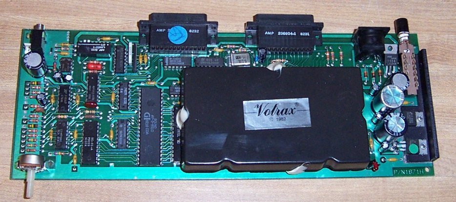
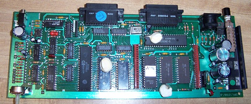
This is the board as it came out of the case. The big black block with the Votrax logo is what I'm going to be working on.
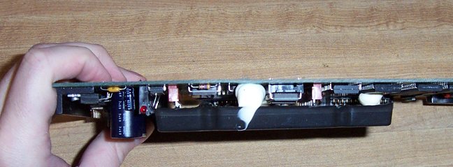
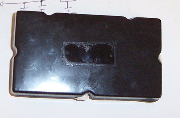
Here's a side view of the block. It's approx. a half inch thick.
This is a close up of the component side. For some reason, they put silicone rubber over the windows of the EPROMs, then potted over top of that. You can see some of the silicone peeking through here and there. There's also some air bubbles and other junk like that.
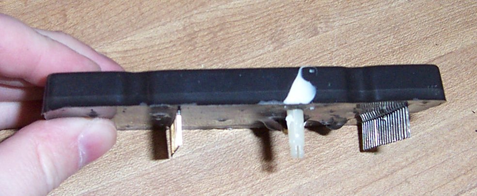
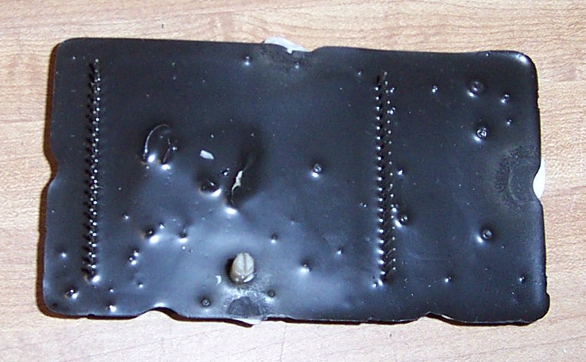
A side view of the removed module.
Top view after the label was removed and saved.
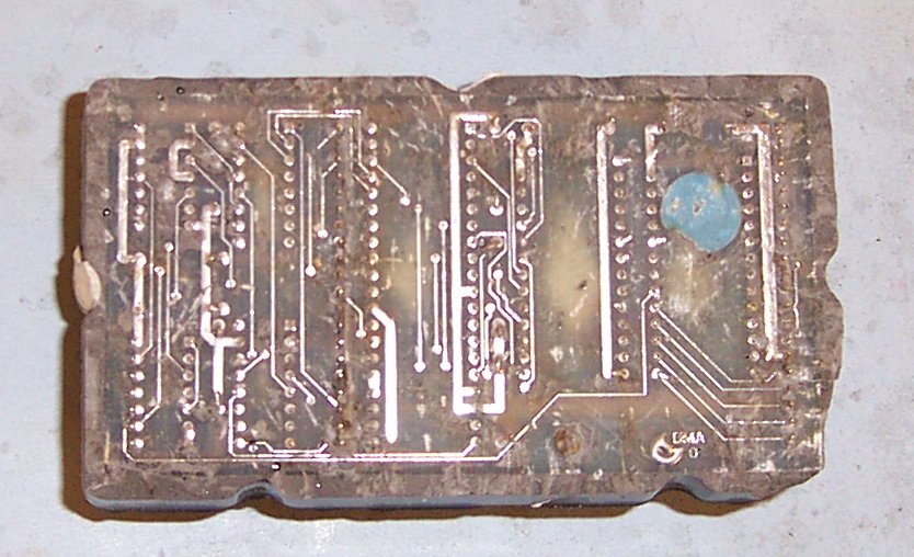
This is a shot of the board without the block on it. There's two RAM chips and an EPROM underneath.
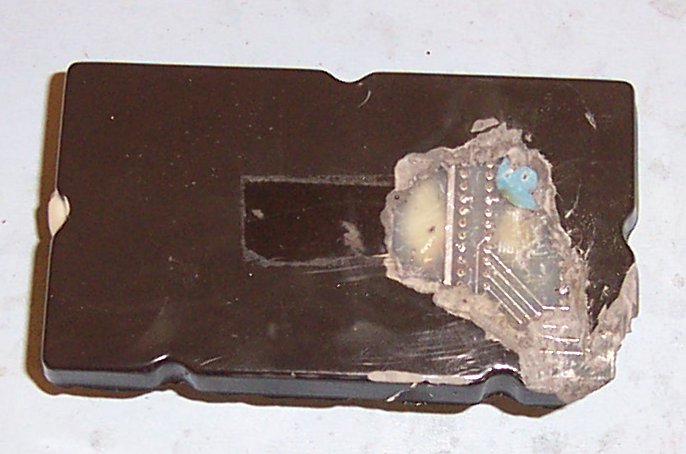
After a little work with the heat gun and knife, the corner of the PCB is visible. I was amused by the blue stick-on label that was on the bottom of the PCB. This was probably to indicate it had been tested and it was OK to pot.
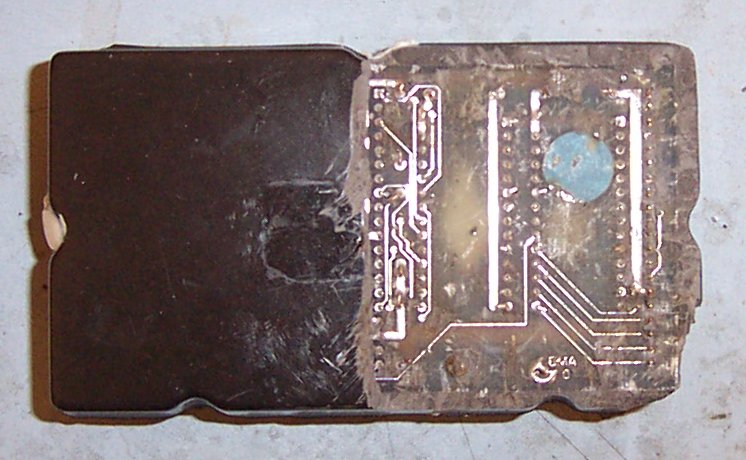
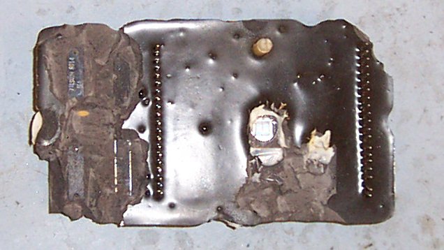
About half the of the epoxy has been removed from the bottom at this point. I can clearly see the bottom of two EPROMs and half of a 40 pin chip.
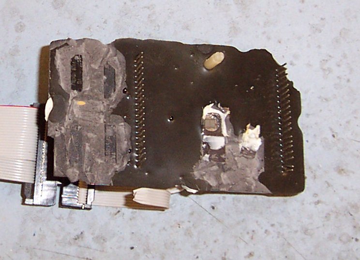
Now, all the chip bottoms can be seen. There's 4 small TTL chips, a Z80, and two 8K EPROMs. The size of the EPROMs was determined by inspecting pin 1, 26 and 27. pin 1 and 27 were pulled high, so it must be 8K or 16K. Pin 26 was not connected, so it is thus 8K. There were two of them on the board for a total of 16K.
Here's a top view of the module. I have removed the epoxy from the top of the 4 TTL chips so I could read their part numbers. They are: 7474, 74139, 7402, and 74367. I also removed the RTV covering the EPROM window. I didn't bother removing the epoxy from the Z80 since I could tell by the connections that it was indeed a Z80.
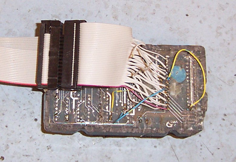
To dump the ROMs, I didn't even have to remove them from the potting compound. I simply cut the power/ground routes going to the Z80, then manually enabled one of the EPROMs, and soldered wires to the bottom. The end of the cable has a DIP plug on it which I just popped into my EPROM programmer. I then dumped the ROM like any other chip. After dumping the first EPROM, I enabled the other ROM with some wires and dumped it. The result is thus two binary files with the ROM contents.
Top view after soldering the wires on.
|
