MMC3
MMC3. Nintendo's most popular mapper chip. It comes in MMC3A, B, and C revisions. The difference is probably something minor like process size.
Registers:
ALL revisions of the MMC3 have been tested and all of them conform to all information below:
MMC3A, MMC3B, MMC3C, and the pirate MMC3 (marked "88") on my pirate SMB3.  This includes
the mapping, IRQs, and WRAM write disable.


8001h, 8000h

Register 8000h is the "control" register, while 8001h is the "data" register.
First, a byte is written into 8000h to select the desired bank register(s).
Then, the desired bank number can be written into 8001h.

8000h:

7  bit  0
---------
CSxx xMMM

C: CHR Address Invert.  When set, does an effective XOR of 1000h with the CHR addresses.

S: PRG ROM swapping control.
0 - 8000-9FFFh and A000-BFFFh can be swapped out while C000-FFFFh is fixed.
1 - A000-BFFFh and C000-DFFFh can be swapped out while 8000-9FFFh is fixed.

E000-FFFF is always fixed to the last bank of ROM.

When S = 0, C000-DFFF will contain the second to last bank of ROM.
When S = 1, 8000-9FFF will contain the second to last bank of ROM.


M: Mode bits

000b 0 - Select 2 1K CHR ROM pages at 0000h in PPU space
001b 1 - Select 2 1K CHR ROM pages at 0800h in PPU space
010b 2 - Select 1K CHR ROM page at 1000h in PPU space
011b 3 - Select 1K CHR ROM page at 1400h in PPU space
100b 4 - Select 1K CHR ROM page at 1800h in PPU space
101b 5 - Select 1K CHR ROM page at 1C00h in PPU space
110b 6 - Select 8K PRG ROM page at 8000h or C000h
111b 7 - Select 8K PRG ROM page at A000h

8001h:

Data register for the desired bank#.

A000h:

7  bit  0
---------
xxxx xxxM

M: Mirroring control

0 - Vertical mirroring
1 - Horizontal mirroring

A001h:

7  bit  0
---------
WRxx xxxx

W: WRAM disable

0 - Disable WRAM (unmaps WRAM totally... reading from WRAM area results in open bus)
1 - Enable WRAM... if present, it is mapped in 6000-7FFFh.

R: WRAM write protect

0 - WRAM is writable
1 - WRAM is readable, but writes do not proceed.

---The Very Last Word on MMC3/6 Interrupts!---

All registers below relate to the interrupts only.

C000h:

This is the IRQ counter's reload value.  The value in this register will be placed into
the IRQ counter proper under *one* condition:

Once the IRQ counter reaches 00h, the NEXT rising edge of A12 will copy C000h's value
into the counter.


C001h:

Writing to this register clears the IRQ counter.  The value on C000h will be copied into
the IRQ counter on the NEXT rising edge of A12.  That means that the value of C000h is
only checked at the very instant of reloading, and C000h's value is not copied when C001h
is written to.  The value written to C001h is irrelevant.

E000h:

IRQ Acknowledge register.  Writing to this register acknowledges an interrupt, and disables
the IRQ flag. The value written is irrelevant.

E001h:

IRQ Enable register. Writing to this register enables the IRQ flag. The value written
is irrelevant.

---

Operation is quite straight forward.  The MMC3 watches A12 on the PPU bus, and decrements
the counter on every RISING EDGE it makes.

Important points:

* The IRQ counter WILL NOT STOP.  It will continue to decrement and reload as long as A12
  on the PPU bus toggles.

* THERE IS NO DIRECT ACCESS to the IRQ counter!

* Writing to E000h will disable the IRQ flag flip-flop, AS WELL AS resetting said IRQ
  flag flip-flop. The IRQ counter is unaffected.

* Writing to E001h will enable the IRQ flag flip-flop. Writing to this register does not
  affect the IRQ counter.

* Writing to C001h will clear the IRQ counter, and it will be reloaded from C000h into
  the IRQ counter on the NEXT rising edge of A12. It will decrement from that point on
  subsequent A12 rising edges.

* Writing to C000h DOES NOT affect the IRQ counter.  When the IRQ counter expires and
  reloads, it will use the new value written.

* Whenever the IRQ counter changes from a non-zero value to 00h, the IRQ flag will be set
  if it is enabled.

* The exact number of scanlines before the interrupt fires is (N+1), where N = the IRQ reload
  value.  2 to 256 scanlines are supported.

* Writing 00h to C000h will result in a SINGLE interrupt being generated on the next rising
  edge of A12.  No more interrupts will be generated until C000h is changed to a non-zero
  value.  The counter is still being reloaded, however, because writing a non-zero value to
  C000h results in it firing an interrupt after the new count expires.

* The IRQ counter WILL NOT DECREMENT AT ALL unless bit 3 OR bit 4 of 2000h on the PPU are
  set! If both of these bits are clear, the IRQ counter will not count no way no how!!!
  If both are set, the counter decrements twice per frame on my MMC3, but it may act
  erratically on your MMC3.  Don't count on this effect occuring.

* For some reason, yet to be determined, if both bits 3 and 4 of PPU register 2000h are
  clear, the IRQ counter will not decrement, even if the PPU address is manually manipulated
  (with 2001h set to 00h to disable rendering) through 02006h. If either or both bits are
  set, the counter will decrement properly if the PPU address is manually manipulated.

Various notes and effects of the IRQ counter reloading stuff:

The IRQ counter reloading has some minor consequences that should be made clear.  Some games
like Megaman 6 and Pinbot use this so emulating properly is important for these games to work.

MM6 will write to E000h to clear the flag, E001h to re-enable interrupts, and finally it will
write to C000h to set up a new time period.  This is legal SO LONG AS C000h is written to
before the next scanline (remember: the counter is reloaded on the NEXT rising edge of A12
after the counter reaches 00h, and thus fires).

I did a little test to determine the effect of C001h on the IRQ counter like so:

First, C000h had 02h written to it.  Toggling A12 3 times resulted in an IRQ being
generated.  The IRQ was cleared, then A12 was toggled 2 more times.  Next, 03h was written
to C000h, C001h was written to, and finally 04h was written to C000h.  A12 was toggled
again and it took *5* counts to flag an interrupt, proving that the value of C000h
is only checked at the time of reloading on the rising edge of A12.  I performed other
tests to corroborate this, and they all passed (i.e. checking to see if the reload happened
on the FALLING edge of A12, etc.)
The Boards: NES-TEROM - Max. 64K PRG, 64K CHRNES-TFROM - Max. 512K PRG, 64K CHRNES-TGROM - Max. 512K PRG, VRAMNES-TKROM - Max. 512K PRG, 256K CHR, 8K WRAM, Battery-backed.NES-TLROM - Max. 512K PRG, 256K CHRNES-TR1ROM - Max. 512K PRG, 64K CHR, 4-screen mirroringNES-TSROM - Max. 512K PRG, 256K CHR, 8K WRAM, Non-battery-backed.NES-TQROM - Max. 128K PRG, 64K CHR, 8K CHR RAMNES-TVROM - Max. 128K PRG, 64K CHR, 4-screen mirroring NES-TEROM - Max. 64K PRG, 64K CHRNES-TFROM - Max. 512K PRG, 64K CHRNES-TGROM - Max. 512K PRG, VRAMNES-TKROM - Max. 512K PRG, 256K CHR, 8K WRAM, Battery-backed.NES-TLROM - Max. 512K PRG, 256K CHRNES-TR1ROM - Max. 512K PRG, 64K CHR, 4-screen mirroringNES-TSROM - Max. 512K PRG, 256K CHR, 8K WRAM, Non-battery-backed.NES-TQROM - Max. 128K PRG, 64K CHR, 8K CHR RAMNES-TVROM - Max. 128K PRG, 64K CHR, 4-screen mirroring
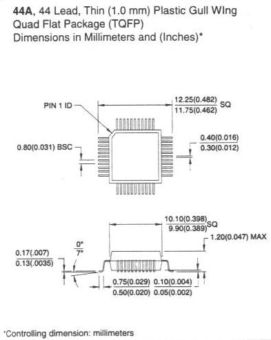
I need the following boards: MMC3 Packaging Information
|